I am an Analog/Mixed-Signal IC Designer with hands-on experience in circuit design across 28 nm–180 nm technologies, including tapeout experience with open-source PDKs such as SKY130, GF180MCU, and IHP SG13G2 (130 nm BiCMOS). I worked as a Research Intern at the LP-CAS (Low-Power Circuits and Systems) Lab, IIT Gandhinagar, under the guidance of Prof. Madhav K. Pathak, where I worked on ring amplifiers and their applications in low-power LDOs. I am currently working in industry on PVT Monitor and Reference IPs in 28 nm CMOS.
These experiences have helped me develop a strong interest in energy-efficient circuit design, research-driven problem solving, and translating circuit-level ideas into practical systems and applications.
Research Interests
High-Speed and Low-Power Data Converters
Biomedical Circuits, Wearable Sensing, and Healthcare SoCs
Ring Amplifiers and other Dynamic Amplifiers
Circuits for AI and AI for Circuits
Algorithm–Circuit Co-Design for Low-Power Sensing and Computation
Neuromorphic and In-Memory Computing
I am particularly interested in energy-efficient analog and mixed-signal circuits for sensing, computation, and data conversion, and in co-designing circuits and algorithms for emerging computing architectures.
I hope to build practical circuit and system-level technologies with real-world impact, especially in healthcare, therapy, sensing, and assistive technologies, where integrated circuits can help improve people's lives.
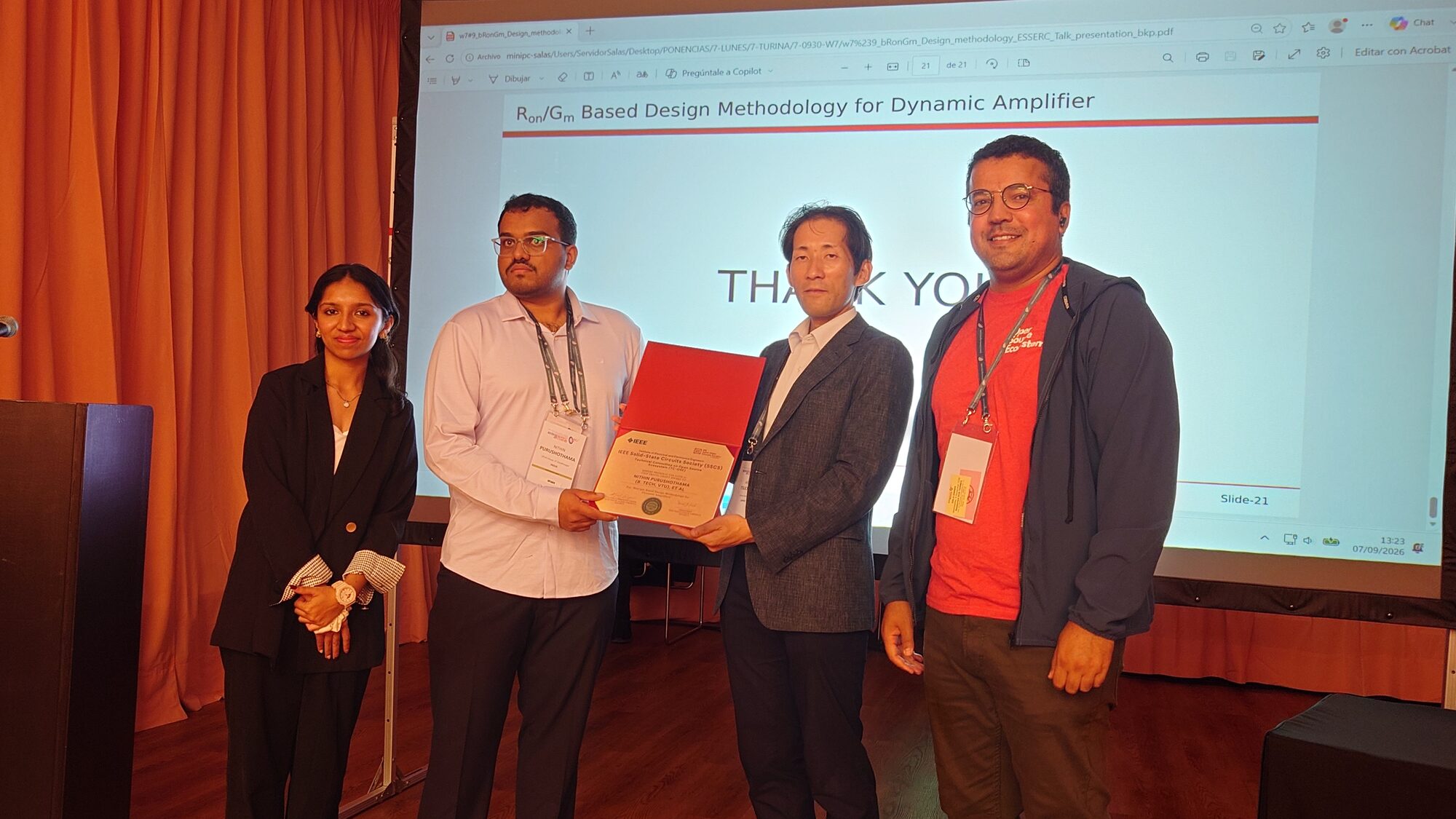
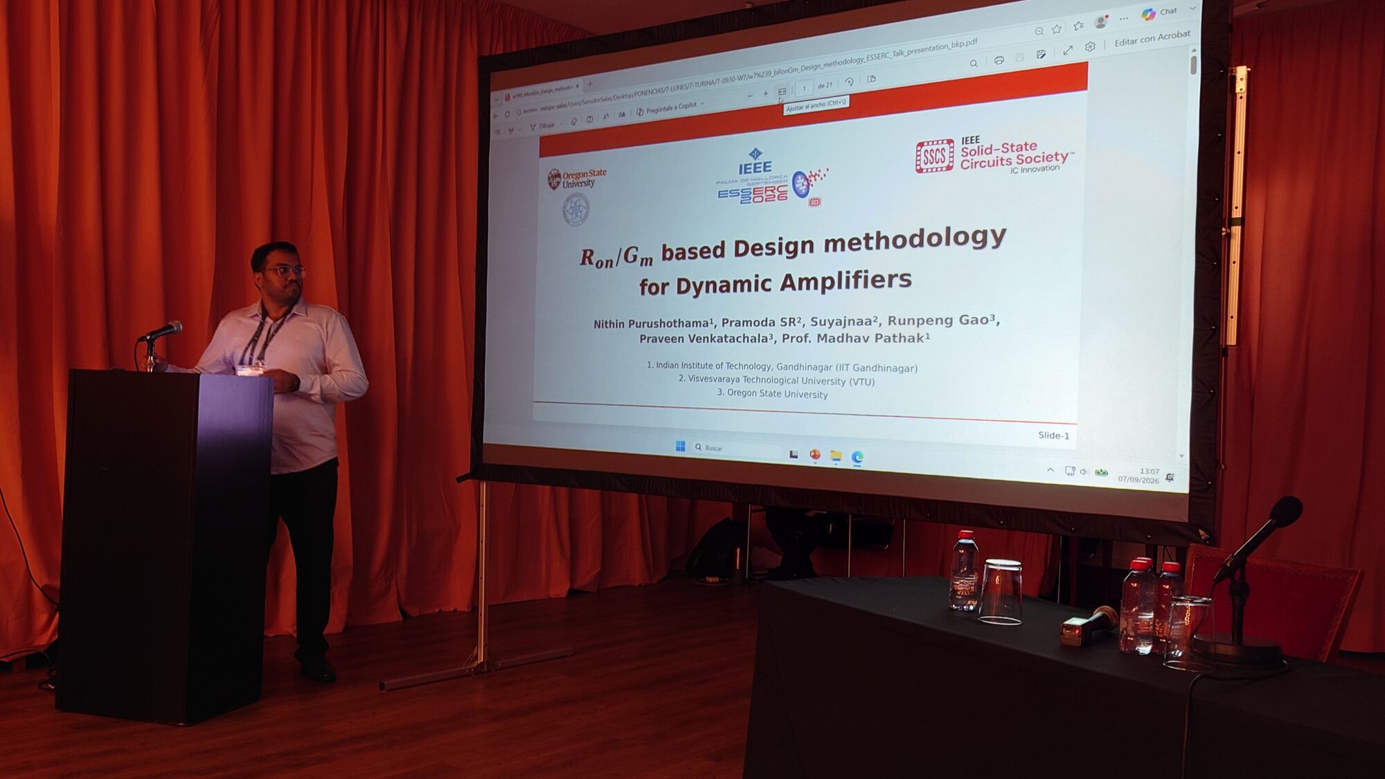
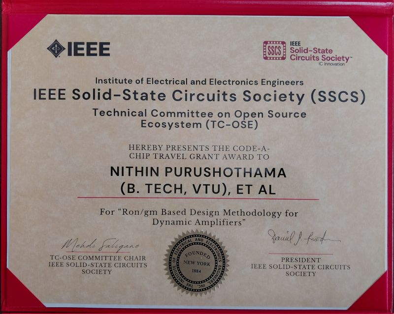
I am also an IEEE SSCS Code-a-Chip Travel Grant Recipient for ESSERC 2026, where I presented my work on Ron/gm based design methodology for dynamic amplifiers.
I am actively seeking PhD positions for Fall 2027.
Block Designs: Designed the Bandgap Core and Reference Analog blocks for the PVT Monitor and Reference IPs in TSMC 28 nm CMOS.
Replaced the BG CORE opamp with a self-biased folded-cascode OTA and a new always-on startup circuit, fixing a common-mode bug that latched the bandgap loop at VDD; reduced 8-bit I-DAC current mismatch to downstream SC-amp and ADC blocks.
Owned REF ANALOG: 5 temperature-compensated high-PSRR reference voltages and 8×200 μA current, adding trim-based programmability to compensate for process and mismatch to meet the ±3% output accuracy specification.
Mapped digital infrastructure from a 16 nm reference IP onto the redesigned 28 nm blocks, enabling block-level reuse and accelerating IP closure.
Block Designs: Designed a 4-input PWM comparator with programmable hysteresis for a multi-phase DC-DC converter SoC in UMC 55 nm CMOS.
Redesigned the comparator to introduce programmable hysteresis at the first stage, eliminating trip-point glitches and reducing propagation delay; reduced power consumption by 30%.
Debugged digital-induced glitches, identifying delay contributions from hysteresis control and de-glitching logic.
2024Class-AB stageAug 2024 – Aug 20251 yr 1 moResearchResearch InternLP-CAS Lab · IIT GandhinagarRon/gm methodology · SKY130 tapeout · ESSERC 2026
Advisor · Prof. Madhav K. PathakDetailsHide
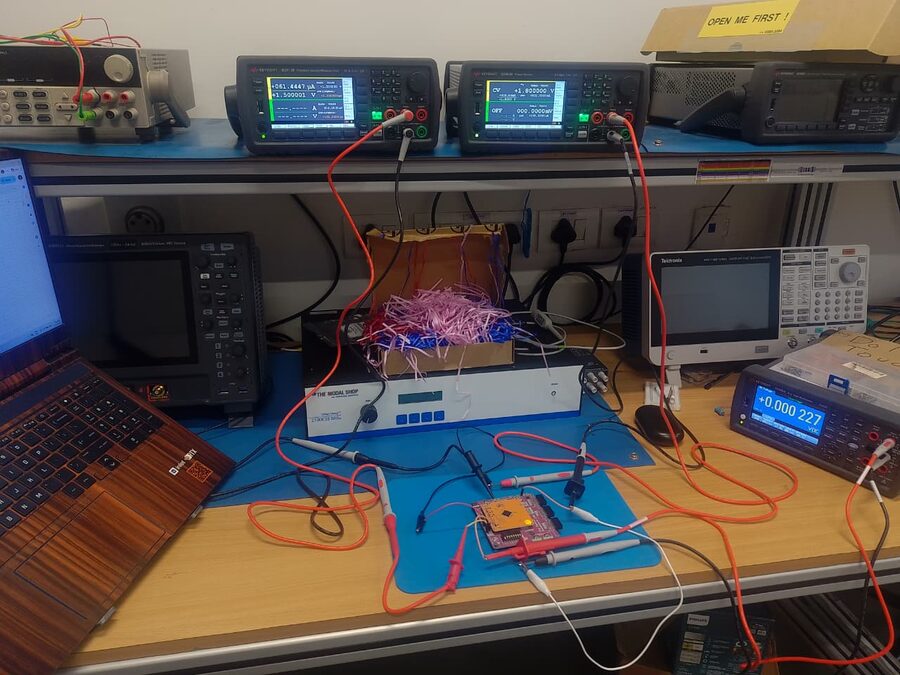
Block Designs: Dynamic Amplifiers and Ring Amplifier-based LDO at LP-CAS Lab, IITGN.
Developed a design methodology for non-linear dynamic amplifiers modelling RC, large-signal, and small-signal settling stages; validated on an inverter-based switched-capacitor amplifier. (Published at ESSERC 2026.)
Proposed a Ring Amplifier-based LDO where the final stage serves as the pass transistor, using adaptive biasing and a deadzone regulation circuit for robust PVT performance.
Proposed a translinear circuit-based MAC architecture for analog neural networks using a digitally controlled subthreshold MOSFET cell with a current-steering DAC for programmable neuron weights.
Served as Teaching Assistant for the IIT Gandhinagar graduate course PMIC Design (EE660).
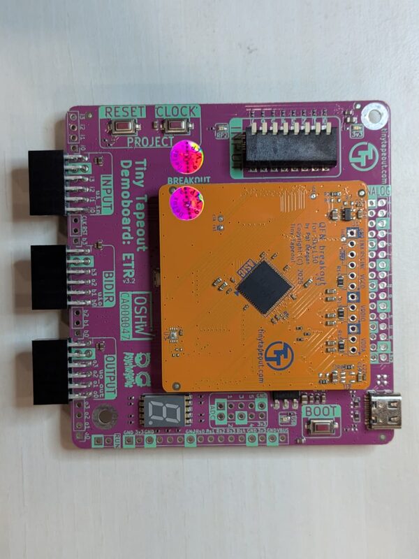
Tapeout: Designed a piecewise-compensated, high-PSRR Bandgap Reference with sub-5 ppm/°C TC in SKY130, including a low-power always-on startup circuit; fabricated through the TinyTapeout SKY130 shuttle.
GeoSat-based satellite communication in the Antenna System for Satellite TTC within C-Band (6 GHz) at the Baseband RF Division, Master Control Facility. Calibrated antenna systems to achieve Cross-Polar Discrimination (XPD) during In-Orbit Testing of GSAT-31.
02
Education
Dec 2021 – Jun 20253 yrs 7 mosBachelor’s
Bachelor of Engineering - Electronics and Communication Engineering
Visvesvaraya Technological University · Bengaluru, India
CGPA8.6/ 10
Courses taken
Circuits & VLSI
Circuit theory
Analog electronics
CMOS VLSI design
Signals & Systems
Signals and systems
Digital signal processing
Control systems
Communication & RF
Analog and digital communication
Microwave and antenna theory
Optical and wireless communication
Digital & Embedded
Microprocessor and microcontrollers
03
Skills
skill project / place domain output applied in
Analog / MS IC designOpen-source EDA & tapeoutResearch & methodologyML & quant finance
Select a node to explore how skills, places, and outputs connect.
·
04
Publications
Conference papers, magazine features, and presentations.
IEEE SSCS Magazine: Ron/gm based design methodology featured within the IEEE SSCS magazine on code a chip competition.
Abstract
This work presents an Ron/gm based design methodology for Inverter based dynamic amplifiers(IBA), addressing a fundamental gap in existing approaches where the large-signal RC settling phase governed by the final stage device ON resistance Ron remains uncharacterized until post-simulation. Unlike the conventional gm/ID methodology, which targets only the small-signal transconductance, the proposed approach simultaneously co-designs both settling phases through pre-characterized device look-up tables (LUTs) derived from parametric SPICE simulations in the IHP SG13G2 130 nm BiCMOS process. These LUTs take into consideration of Ron/gm as a function of device geometry, bias, and process corner, making worst case corner behavior and valid bias deadzone boundaries directly readable at the design entry stage without iterative simulation. A head to head comparison with the gm/ID methodology confirms that the Ron/gm approach achieves equivalent settling accuracy while substantially reducing design cycles and providing more useful information regarding deadzone bias requirement by surfacing process-corner sensitivity upfront.
Cite this
Nithin P, Pramoda SR, Suyajnaa, Runpeng Gao, Praveen Kumar Venkatachala, and Madhav Pathak, “Ron/gm based design methodology for dynamic amplifiers,” IEEE Solid-State Circuits Magazine, Dec. 2026, to appear.
@article{p2026rongm,
  author  = {Nithin P and Pramoda SR and Suyajnaa and Runpeng Gao and Praveen Kumar Venkatachala and Madhav Pathak},
  title   = {{$R_{on}/g_m$} Based Design Methodology for Dynamic Amplifiers},
  journal = {IEEE Solid-State Circuits Magazine},
  year    = {2026},
  month   = dec,
  note    = {To appear}
}
Design and comparison of analog multiplier circuits for low-power pre-ADC sensor processing, power management, and analog neural networks using translinear and linear MOSFET-based MAC architectures.
Abstract
Multiplication is a key computational step in analog signal processing circuits used in various low-power applications such as pre-ADC sensor data processing, controllers for power management circuits, and analog neural networks. This paper compares two analog multiplication approaches: a Trans-linear Loop based design and a Linear MOSFET based design. The operating principles, voltage and current ranges, and design trade-offs of both circuits are analyzed. Implementations are carried out in the open-source SKY130nm CMOS process and verified through simulations. The trans-linear circuit consumes less than 21.53 µW, while the Linear-MOSFET based circuit consumes 39.78 µW. Guidelines for circuit optimization are provided, highlighting trade-offs in accuracy, power consumption, and area overhead. Impact of device mismatches in the multiplier circuits is evaluated using Monte Carlo simulations. Simulation results demonstrate the performance and limitations of each approach, providing a reference for the design of analog multipliers.
Cite this
Nithin P and Madhav Pathak, “Analog CMOS multiplier circuits: design and comparative analysis,” in IEEE ICEE 2025, Feb. 2025.
@inproceedings{p2025multiplier,
  author    = {Nithin P and Madhav Pathak},
  title     = {Analog {CMOS} Multiplier Circuits: Design and Comparative Analysis},
  booktitle = {IEEE ICEE 2025},
  year      = {2025},
  month     = feb,
  url       = {https://ieeexplore.ieee.org/abstract/document/11409824}
}
ESSERC 2026 · Palma de Mallorca, Spain · Sept 2026
Recipient of the IEEE SSCS Code-a-Chip Travel Grant Award. Presented the work on a Ron/gm-based design methodology for dynamic amplifiers at the award ceremony.
Abstract
This work presents an Ron/gm based design methodology for Inverter based dynamic amplifiers(IBA), addressing a fundamental gap in existing approaches where the large-signal RC settling phase governed by the final stage device ON resistance Ron remains uncharacterized until post-simulation. Unlike the conventional gm/ID methodology, which targets only the small-signal transconductance, the proposed approach simultaneously co-designs both settling phases through pre-characterized device look-up tables (LUTs) derived from parametric SPICE simulations in the IHP SG13G2 130 nm BiCMOS process. These LUTs take into consideration of Ron/gm as a function of device geometry, bias, and process corner, making worst case corner behavior and valid bias deadzone boundaries directly readable at the design entry stage without iterative simulation. A head to head comparison with the gm/ID methodology confirms that the Ron/gm approach achieves equivalent settling accuracy while substantially reducing design cycles and providing more useful information regarding deadzone bias requirement by surfacing process-corner sensitivity upfront.
Cite this
Nithin P, Pramoda SR, Suyajnaa, Runpeng Gao, Praveen Kumar Venkatachala, and Madhav Pathak, “Ron/gm based design methodology for dynamic amplifiers,” presented at ESSERC 2026, Palma de Mallorca, Spain, Sep. 2026.
@misc{p2026rongmesserc,
  author       = {Nithin P and Pramoda SR and Suyajnaa and Runpeng Gao and Praveen Kumar Venkatachala and Madhav Pathak},
  title        = {{$R_{on}/g_m$} Based Design Methodology for Dynamic Amplifiers},
  howpublished = {Presentation at ESSERC 2026 (IEEE SSCS Code-a-Chip Travel Grant), Palma de Mallorca, Spain},
  year         = {2026},
  month        = sep,
  url          = {https://colab.research.google.com/drive/1q6r7tg8RoyLBaMS3b7EONwkPCBzEM2c1}
}
IEEE Solid-State Circuits Society (SSCS) – Open-Source Ecosystem (TC-OSE)
Grant$5,000
Awarded for “Ron/gm Based Design Methodology for Dynamic Amplifiers”, a notebook demonstrating a novel design methodology for inverter-based dynamic amplifiers on IHP SG13G2 using open-source EDA tools. Award ceremony at ESSERC 2026, Palma de Mallorca, Spain.
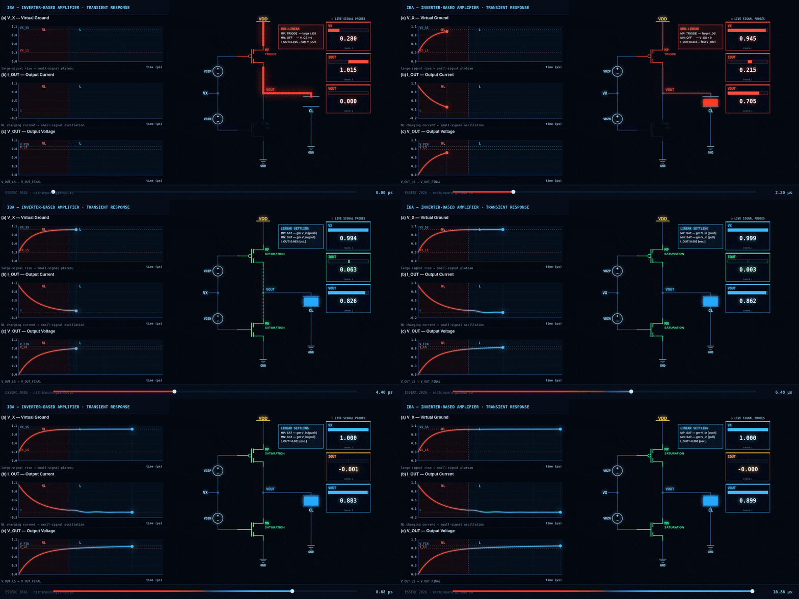
Dynamic amplifiers exhibit two distinct settling regimes: an initial non-linear, large-signal phase dominated by the transistor on-resistance Ron, followed by a linear, small-signal phase governed by gm. During the first phase, the output rapidly moves toward its final value with an effective time constant
τLS ≈ RonCload,
while the final settling and small-signal bandwidth are determined by
τSS ≈ Cload / gm.
Conventional gm/ID-based design methods are effective for small-signal optimization, but do not directly constrain signal-dependent Ron, required voltage swing, or the resulting large-signal settling behavior. Consequently, a design with sufficient gm at nominal conditions can still exhibit slow settling at process corners where Ron increases.
We therefore propose a Ron/gm-based design methodology that explicitly allocates the settling-time budget between the two regimes. For a target settling time Tsettle, a fraction α is assigned to small-signal settling and (1 − α) to large-signal settling:
The required gm is then selected as the larger of the settling requirement and the application bandwidth requirement,
gm = max( gm,min , 2π fBWCload ).
This provides a direct connection between Ron, gm, Cload, bandwidth, and settling time, allowing the unit cell to be sized independently of the final load and subsequently scaled by a multiplier M:
Ron → Runit / M , gm → M gm,unit , ID → M ID,unit.
Importantly, the proposed approach separates the two design knobs. The signal-path transistor width is primarily fixed by the required Ron, while gm can be further tuned through a replica bias path by adjusting its current and device sizing across process corners. This allows small-signal bandwidth to be corrected without altering the signal-path Ron and therefore without compromising large-signal settling.
The resulting Ron/gm metric provides a pre-simulation design and corner-verification framework for dynamic amplifiers, exposing slow-corner settling mechanisms that can remain hidden in a conventional gm/ID-only design flow.
expand
IBA transient response: Non-linear settling (red) → Linear settling (blue) ·
IHP SG13G2 130 nm BiCMOS ·
Ron/gm methodology
Performance Summary and Comparison with State-of-the-Art
Pre-simulation Vbias predictions were within ±75 mV of post-simulation values; Ipeak predicted within ~15%.
† J. Conrad et al.: "Unfortunately, Section II-B is not really practical for designing a RAMP… This makes a design-by-equation cumbersome and not realizable." [TCAS-I 2020, Sec. II-C]
‡ J. Conrad et al.: "PVT variations are not encountered during the circuit optimization, because this would require many transient simulations to evaluate one iteration of the optimizer." [TCAS-I 2020, Sec. V-E]
§ Deadzone bias values read from the Vbias vs. log(Ron/gm) LUT plot at Ron/gm = 50 × 106 (per device, post-multiplier), Ibias = 0.5 μA (unit cell), Ibias = 2 μA (Overall IBA).
¶ J. Conrad et al.: "the optimizer goal for the accuracy was readjusted ×4 smaller, i.e. 0.25 for the cost function." [TCAS-I 2020, Sec. IV-B.3]
** J. Conrad et al., Table II: 180 nm power cost function = 12.99 (target: 1.0), failing the power constraint by 13×.
Implemented higher-order curvature correction using piecewise compensation technique to compensate for BJT non-idealities in Bandgap; achieved 4.4 ppm/°C Temperature Coefficient.
Improved PSRR via cascode current mirrors; conducted full PVT corner verification across process, voltage, and temperature.
Designed a POR circuit in SKY130 PDK using a current comparator with PMOS/NMOS current mirrors for supply threshold detection; VPOR asserts Enable at VDD = 1.5 V across PVT corners.
Open-source Python tools for analog IC design automation: PVT sweep framework for NGSpice: automated metric extraction, comparison plots across corners.
SPICE-to-area estimation tool using Magic VLSI for pre-layout floorplanning.
Designed a PVT-robust Ring Amplifier in IHP SG13G2(BiCMOS); Deadzone regulation circuit where negative feedback controls third-stage quiescent current across process corners.
Dynamic error analysis covering RC, large-signal, and small-signal settling regimes. Validated performance in a switched-capacitor amplifier testbench.
Designed a subthreshold-based Voltage reference current with current matching between a diode-tied NMOS and a native NMOS load transistor for reference generation without a dedicated bias circuit.
Achieved 60 ppm/°C TC across process corners with total power ≤ 2 pW.
Fully differential OTA in SKY130 with PMOS differential pair and NMOS load; buffer-based common-mode sensing stabilizes output common-mode voltage for larger gain.
Unified gm/ID explorer for three open-source PDKs: interactive MOSFET characterisation curves (gm/ID, fT, gm/gds and more versus VGS, Vov and channel length) for gm/ID-based analog design.
Quantitative analysis of seven INR currency pairs (EUR, USD, GBP, JPY, CNY, SGD, HKD) for timing a transfer: ensemble forecasts (ARIMA, Holt-Winters, Monte Carlo), technical indicators, risk and seasonality, on ECB rates refreshed daily by a data bot.
Live feed of the newest papers and posts in AI, finance and chip design: arXiv, Hugging Face trending papers, the latest IEEE JSSC, TCAS, TVLSI, TCAD and IEEE Micro articles, Semantic Scholar and research blogs, refreshed every 3 hours, with an optional Claude-powered paper explainer.
Interactive signal-path explorer for a secure delta-sigma sensor front end, running a behavioural model live in the browser. Compares the ESSERC'25 S-DSM baseline with a proposed SRAM-PUF + fuzzy extractor + NLFSR scheme, and lets you probe every block, from the modulator bitstream to key recovery, under attack scenarios.
31 public repositories ·
81 stars -
more on GitHub.
07
Quantitative Finance
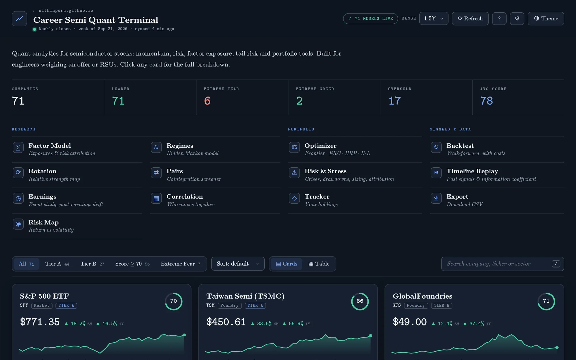
Outside of circuit design, my primary interests lie in macroeconomics and data-driven quantitative analysis of businesses and financial markets, particularly the use of machine learning and large-scale economic and financial datasets to study economic trends, business decisions, and investment opportunities.
Implementation of standard risk metrics including Value-at-Risk (VaR), Conditional VaR (CVaR), Beta, Sharpe ratio, and Sortino ratio for portfolio performance evaluation.
08
Hobbies
Reading history
Especially classical history and the Roman Empire.
Book recommendations
Written by Caesar
The Gallic WarCommentarii de Bello GallicoJulius Caesar
The Civil WarCommentarii de Bello CiviliJulius Caesar
Ancient Roman historians
The History of RomeAb Urbe ConditaLivy
The AnnalsAnnalesTacitus
The Twelve CaesarsDe Vita CaesarumSuetonius
The Conspiracy of CatilineDe Catilinae ConiurationeSallust
On the Roman Empire
SPQR: A History of Ancient RomeMary Beard
The History of the Decline and Fall of the Roman EmpireEdward Gibbon
Non-dualistic philosophy
Advaita Vedanta - the teaching of non-duality.
Book recommendations
Works of Adi Shankaracharya
VivekachudamaniThe Crest-Jewel of Discrimination
Atma BodhaKnowledge of the Self
Upadesa SahasriA Thousand Teachings
Bhaja Govindam
Brahma Sutra BhashyaCommentary on the Brahma Sutras
From Sringeri Sharada Peetham
Dialogues with the GuruTalks of Sri Chandrasekhara Bharati Mahaswamigal
Yoga, Enlightenment and PerfectionSri Abhinava Vidyatheertha Mahaswamigal